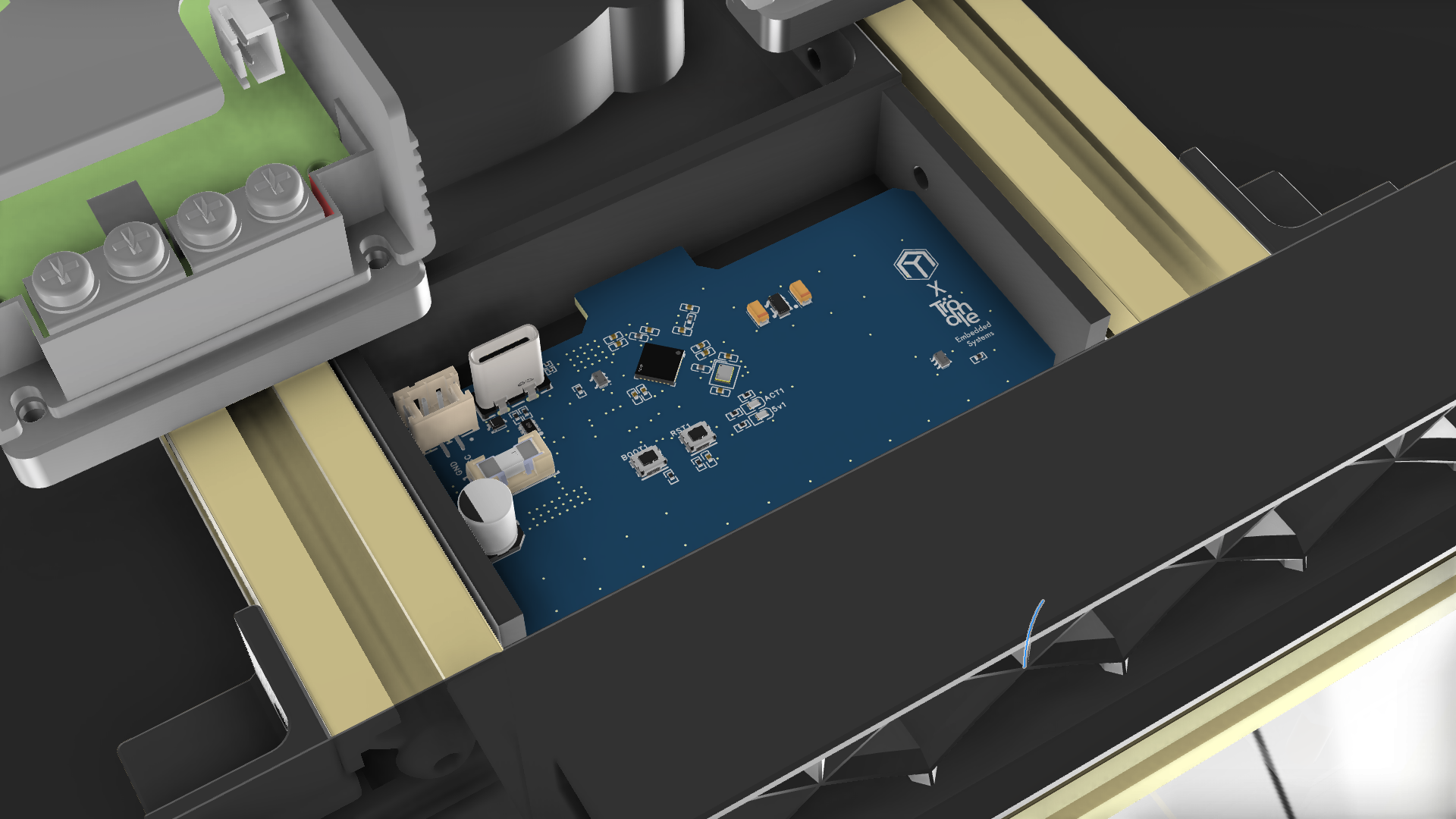
AT2 WLED PCB
Four-layer control board driving addressable LEDs for decorative and functional feedback.

 View on GitHub
 Buy on TES-shop
AT2 3D Printer LED Bed PCB
A compact, four‑layer control board that sits beneath the AT2 print bed and drives addressable LEDs for decorative and functional feedback.
Key Features
- ESP32-C3FH4 MCU with integrated PCB antenna (Wi‑Fi + BLE)
- Two independent LED outputs
- Logo chain (AT2 logo)
- Status bar (progress, time remaining, temperature alerts)
- 3.3 V → 5 V level‑shifters on each data line
- 3 A Littelfuse on the 5 V rail
- SMD JST‑XH connectors for plug‑and‑play wiring
- 4‑layer stack‑up with dedicated VCC & GND planes for low noise
Connectors & Pin‑out
| Label | Type | Description |
|---|---|---|
| VCC | 2‑pin JST‑XH | 5 V fused supply input |
| GND | 2‑pin JST‑XH | GND Input |
| LED_ACT | SMD | Status LED |
| BOOT1 | SMD button | Hold BOOT low for ESP32 flash mode |
| RST1 | MD button | Manual reset to ground the EN pin |
Power Architecture
- Operates from an existing 5 V supply (no on‑board buck converter)
- 3 A LittleFuse protects the entire board
License
Released under the MIT License – see LICENSE.